Home>>User Support>>DDC using FPGA
Digital DownConversion (DDC) using FPGA
Introduction
A fundamental part of many communications systems is Digital DownConversion (DDC). This allows a signal to be shifted from its carrier (or IF) frequency down to baseband. The technique greatly reduces the amount of effort required for subsequent processing of the signal without loss of any of the information carried.
You would never consider using a DSP like the C6000 for DDC. Historically it has been performed in analogue before digitising the baseband signal for the DSP.
The HERON-FPGA family is ideal for many of the building blocks of digital communications. Providing large easily-programmed gate arrays, often combined with interface elements like ADC or DACs, they can be used to implement many system components.
This note describes how a DDC can be implemented in the HERON-FPGA or HERON-IO family. While the technology looks complex, it is actually very simple, and can be implemented extremely quickly.
Theory of operation is not addressed here – there is a separate paper from Hunt Engineering which introduces the concepts of the DDC.
See also the very good article by Ray Andraka (Andraka Consulting Group, Inc) on the subject of DDC with FPGAs.
We provide demo/frameworks of a DDC in a HERON-IO2 and a HERON-IO5 that are similar to the discussion below.
What Are We Implementing?
Essentially, a DDC comprises an oscillator, generating a quadrature signal; a mixer, which multiplies the incoming signal by the local oscillator; and then filtering. This combination frequency-shifts the signal. Typically the frequency shift is the frequency of the local oscillator. Many systems will try and match the local oscillator to the carrier, shifting the received signal back to baseband.
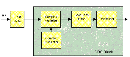
A Theoretical DDC Block
Diagram
Getting the Signal from the ADC
The ADC will be implemented externally to the FPGA. If you’re using a module with an integrated ADC, the Hardware Interface Layer supplied will provide a macro for interfacing to the ADC converter(s). If the module does not have an ADC, you will need to gather the data using the FIFO interfaces – again using macros from the library supplied.
The details of this are module dependent so are not discussed further here.
Implementing The Local Oscillator & Mixer
This is the first stage of the DDC. The local oscillator is a quadrature oscillator, generating a highly accurate and stable version of the carrier. The Xilinx "Core Generator" tool offers a "Direct Digital Synthesiser" or DDS which will implement this function.
There are a number of parameters to consider:
- How accurate should the frequency control of the oscillator be? With a digital oscillator, you can specify very fine control – at the expense of increased FPGA utilisation.
- Do you need to program the phase of the oscillator? To what resolution?
- How much noise can you tolerate in the oscillator’s output? Any noise will be passed through the mixer into the DDC’s filters, and will add to the system’s noise floor. You may want to analyse this.
With this information, you can move to generating a core with the Xilinx toolset. The best approach is to generate the biggest DDS you can squeeze into the FPGA, but record the parameters you use. If you need to optimise the design later, you can regenerate the core with (for example) reduced frequency accuracy to increase speed.
Similarly, the mixer is implemented as a pair of hard-coded multipliers. It is usually not worth trying to implement the mixer in a single multiplier. Ensure that the outputs are registered, and select the pipelined multiplier option. It should now be a simple matter to connect the oscillator to two of the multiplier inputs, while the ADC can go on the other input.
Filtering & Decimation
There are two main classes of DDC – wideband and narrowband, differentiated by their decimation ratios. As a rough guide, if the decimation ratio is less than 32, consider the DDC wideband; if 32 or more, the DDC is narrowband.
The filtering we will perform is different for narrowband or wideband, so is tackled separately. However, the decimators can be treated identically for wideband or narrowband systems.
Note also that in some systems it may make sense to combine wideband and narrowband DDCs. For example, in a GSM system which uses 8 carriers, a wideband DDC could be used to shift the carriers down to a moderate frequency. This could be done using a simple oscillator – no complex components. 8 narrowband DDCs could then be used to select the individual carriers. The theory is the same…
Filtering for Wideband DDCs
With a wideband signal, we are typically reducing the sampling rate by a small amount, and the data output rate is large. Note that the output rate of a wideband DDC should be checked as part of your overall system design. In some systems that data rate will be significant, and could saturate a DSP processor – if that is meant to be receiving it.
The main challenge of a wideband receiver is getting enough processing to filter the signal. All the processing is performed at a fairly high rate, often 20-40MHz. Because of this, the filters tend to be very gate-intensive; a single wideband channel will typically consume more of an FPGA than several narrowband channels.
Each design has different requirements. However, the following is a rough guide to implementing the filter. The filter is best implemented as an FIR, and in fact the best approach is to use a multi-rate FIR. This may sound complex, but in fact a multi-rate FIR is simply an efficient way of implementing large filters with decimation. Imagine we need to implement a large filter at a high sampling rate, before decimating the signal. We could implement a 128-tap filter at 100MHz, but this would require a lot of multipliers and a huge FPGA.
However, suppose we split the filter. The first filter can perform enough filtering to allow us to perform some decimation. The second filter is now operating at a much reduced sampling rate.
Typically by splitting the filter in this way we can reduce the number of taps in the filter, and reduce the sampling rate that some of these taps operate it. Both reduce the amount of FPGA resource we require to build the filter.
So, to implement your filter: start with a simple FIR. This stage should have a small number of taps - if you are operating at a high sampling rate, each FPGA multiplier will implement a very small number of taps. Use symmetric FIRs here – the processing load is about half a non-symmetric filter, and the core generator provides this as an option. Regardless of which FPGA you are using, this stage will take a lot of silicon! The filter’s bandwidth should match the output bandwidth of the DDC, but don’t worry too much about the filter’s performance – later filters will improve this.
(Note: the output bandwidth is the band that we’re interested in – typically only a few hundred KHz wide)
Immediately after this filter, decimate the signal by 2, and implement a larger filter. Again, the filter’s bandwidth should match the DDC output bandwidth. This will improve the response of the first filter. You can afford to have more taps in this stage, as the sampling rate is lower.
If you are operating a low decimation ratio, this could be all you have to do. That means that these filters have to have more taps than if we can use an additional stage. Experiment by trying cascades of filters with varying numbers of taps – you will probably have to do this iteratively, using the Xilinx tools to try several different scenarios.
For higher decimation ratios (e.g. 8 and up), you can afford to use a third stage filter. This can have significantly more taps than the first two, as each multiplier here can implement at least 4x as many taps as in the first stage. Again, you will want to experiment with the layout of the filters to see what gives best performance.
Filtering for Narrowband DDCs
Narrowband DDCs have a different set of challenges. With these, we need filters that can allow large decimation ratios without consuming too much of the FPGA.
A very useful filter here is the Comb-Integrator Cascade filter, or CIC filter. This filter has remarkable properties – it can implement decimation within the filter, and it provides a steep cut-off for relatively few stages. Best of all, it is implemented using only adders and delays, which makes it very well suited to FPGA implementation.
The CIC has one failing – it has a lot of "droop" in its passband, and serious ripples in its stopband. However, we can compensate for these with additional filtering of its output.
Because of the need for additional filtering on a CIC’s output, it is at its best with large decimation ratios. The larger the decimation ratio, the smaller the overhead of the filters used to compensate for the CIC. This makes it unsuitable for the wideband DDC we looked at earlier as the compensation filter becomes significant. However, for the narrowband DDC, it is ideal as a first stage.
We would then follow that with a multi-rate FIR filter, as with the wideband DDC. Now, we can use as many taps as a single multiplier will allow. Generally a two-stage FIR works well, decimating by 2 between the stages. For many applications, 23 taps will work well in the first filter, and should be realisable with a single multiplier design; while 63 would be ideal in the second. Again, use symmetric FIRs to reduce the processing load.
Designing the Filters
Everybody has their own favourite way of designing filters. Some will simulate the filters in Matlab or one of the other commercial packages; others may use one of the on-line tools, such as the filter design package at http://www.nauticom.net/www/jdtaft/. In all cases, studying the datasheets of commercially available DDC devices can give some guidance – many of these detail the procedures for designing a DDC filter chain, and often list the coefficients. These filters may be copyright protected, but they will give good guidance on design.
The CIC doesn’t really need to be designed – you just need to calculate the word length required in the integrator’s accumulators. Be careful here – the CIC needs surprisingly big accumulators due to huge wordlength growth. The size of the accumulator is dependent on the number of stages in the filter and the decimation ratio – check the references if you need help on this.
Implementing the Filters
Once you have the filters designed, implement them. For the CIC, it is best to implement this from scratch – although there is a 5-stage CIC included in the example for this white paper. Be aware that the CIC’s wordlength is dependent on the decimation ratio though – the example CIC will overflow on larger decimation ratios. It is easily modified for longer wordlengths.
For the FIRs, we will again us the Xilinx Core Generator tool – this allows you to specify the parameters of the filter and it will generate an FPGA core to match. Make sure you keep a record of the settings you use – this may well be an iterative process if you need to optimize the design for speed or size, and knowing what you asked for will help immensely!
The Xilinx tool will even generate decimating FIRs for you. Specify the decimation ratio, and the output will signal a valid sample at the decimated output rate – an incredibly powerful tool for this type of work.
Note that the Xilinx FIR tool also allows you to specify the number of clocks per output sample. Make sure you specify the maximum number of clocks; that way, the tools will be able to use the least possible amount of FPGA resource to implement your filter. Note that in a multi-rate filter, the later stages will have more clocks per output than the early stages!
Once the filters have been generated, they’ll be in the library for your Xilinx design. Build up the DDC’s processing chain. It is worth registering the data along the chain (specify the "register output" option on the filters). Make sure the system clock is connected to all elements – we’ll see how to control the DDC in just a moment.
The Decimator
The final decimator can be implemented within the last FIR stage, if the decimation ratio is an integer. To do this, simply specify the required decimation ratio as part of the filter design.
However, you may require a non-integer decimation ratio, or you may require a variable decimation ratio. In these cases, we must treat the decimator as a separate block.
For non-integer decimation, run the FIR Core Generator one more time. Select an interpolating filter; this will automatically increase the sampling rate by the given amount. Place this in your design.
The decimator can now be implemented as a register & counter. An example of this type of decimator can be found in the middle of the CIC filter used in this example.
The Core Generator DDC
The discussion above helps you to understand how the DDC is designed and works, but in fact there is a DDC block in the core generator. You enter much the same information as you would into the individual blocks but what results is a single Core generator block that probably uses less real estate than the discrete one. If your design goals can be met with this Coregen block then you should certainly use it. If it limits what you need to do then you can implement your DDC in separate blocks.
We provide worked examples of implementing a DDC in a HERON-IO2 and a HERON-IO5