Home>>User Support>>DDS using FPGA
Direct Digital Synthesis (DDS) using FPGA
Introduction
The HERON-FPGA family is ideal for many of the building blocks of digital communications. Providing large, easily-programmed gate arrays, often combined with interface elements like ADC or DACs, they can be used to implement many system components.
A popular requirement is for Direct Digital Synthesis (DDS), to generate high-frequency waveforms without any load on the DSP processors in the system. In many cases the waveforms generated are modulated by signals from baseband processing, for example in transmission systems. This is simple to achieve, as we explain in this note.
What Are We Implementing?
Essentially, a DDS comprises one or more "digital oscillators". Each of these oscillators generates a sine wave. This can be modulated in phase, frequency or amplitude.
The oscillators are usually all clocked from a common clock. This means they can all be synchronised; for example, two oscillators can be used to generate a quadrature carrier with very precise 90-degree phase separation, or multiple carriers can be generated with very tight control over the phase relationships.
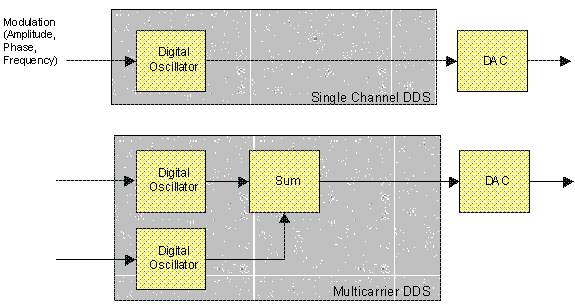
For many systems, each signal would be output to a DAC. This brings the prospect of building multi-channel generators, with each oscillator directly generating an analog output.
In contrast, multiple-carrier communications systems (like GSM) would typically sum the oscillator outputs together, before passing the single output signal to the DAC.
How’s It Done?
There are many ways of achieving this, but one of the simplest is to use a pointer into a sine-wave table. With each sample, the pointer is incremented; when the pointer reaches the end of the table, it is reset back to the beginning.
This is the basis of a look-up table DDS, which is well suited to being implemented in a Xilinx array. However, there are a few added complications for a real DDS:
- We need a simple way to reset the table pointer. Typically this is achieved by making the table size a binary multiple (such as 16, 32, 64, 128….). If this is the case, the pointer will roll over automatically.
- The overall size of the table is dependent on the number of entries, and the resolution of those entries. Optimum performance may not be achieved with large samples – it may make sense to reduce the sample resolution but increase the number of samples, as we’ll see later.
- The table need not be a full sine wave – in fact, a quarter is sufficient. However, for smaller tables, the overhead in performing the maths on the pointer and sample may exceed the benefits of reducing the table.
- The increment of the pointer cannot be an integer; if it was, the frequencies generated would be limited to fractions of the sampling rate.
With this in mind, we can see that the pointer has two parts – an integer part, and a fractional part. The integer part is used to address the table, while the fractional part allows us to generate non-integer fractions of the sampling rate. Thus, if a 32-bit pointer is used, with a 256-entry table, we’d have a pointer with 8 bits of integer, plus 24 bits of fraction. The more bits we have defining the fractional part, the greater the frequency resolution.
Following on from this, we can also see that for non-integer values of the pointer, the sample read from the table will have some error. For example, if our pointer is 18.4, we will read value 18; where in fact we should have a value somewhere between value 18 & value 19. This generates noise on the output waveform.
In fact, noise on the output comes from two sources – errors brought about by the limited resolution of the table entries, and errors caused by reading a value between two table entries. The latter tends to predominate for small tables – don’t assume you must use 16-bit samples, there may be far more benefit in increasing the number of samples in the table!
Introducing Modulation & Combining Carriers
Frequency modulation is achieved by simply adding the modulated signal to the "pointer increment" value. This can be done on a per-cycle basis. Phase modulation is performed by adding the modulating signal as an offset to the pointer before performing the table lookup. Amplitude modulation is performed by multiplying the modulating signal with the DDS output. All of these are simple to implement.
Summing multiple carriers is equally easy – just add the outputs of several DDS modules together. It may be possible to use pipelined adders for this, but do consider the number of pipeline delays each channel is subjected to – otherwise some channels may be delayed more than others, and lose synchronisation.
Designing a Table-Driven DDS
Now the hard bit! The DDS is available as a core within the Xilinx core generator tool. This will allow you to create a DDS core with one or two channels in a matter of seconds. Multiple channels can be created by placing multiple single or dual channels within the FPGA. Cores can be generated that load new frequency or phase values on every sample if required.
Reducing the Output Noise
There are several approaches that can be used to reduce the noise generated at the DDS output. The first is to filter the output, which may be practical in some circumstances – but note that the filter will probably have a fixed frequency, while the DDS is extremely "frequency agile". Another approach is to add jitter (a small amount of random noise) to the frequency and/or phase values used – this is probably better as it does not restrict the DDS to a pre-set frequency range. Either of these may be used to good effect with the core generator’s basic DDS module, and they may of course be combined.
Other approaches include interpolating between table entries, but this would require a custom core to be generated. Not a big job, but it would take hours rather than the seconds required to build a standard DDS!
Getting the Signal to the DAC
The DAC will be implemented externally to the FPGA. If you’re using a module with an integrated DAC, the support library supplied should provide a macro for interfacing to the DAC converter(s). If the module does not have a DAC, you will need to transmit the data to other modules using the FIFO interfaces – again using macros from the library supplied.
The details of this are module dependent so are not discussed further here.