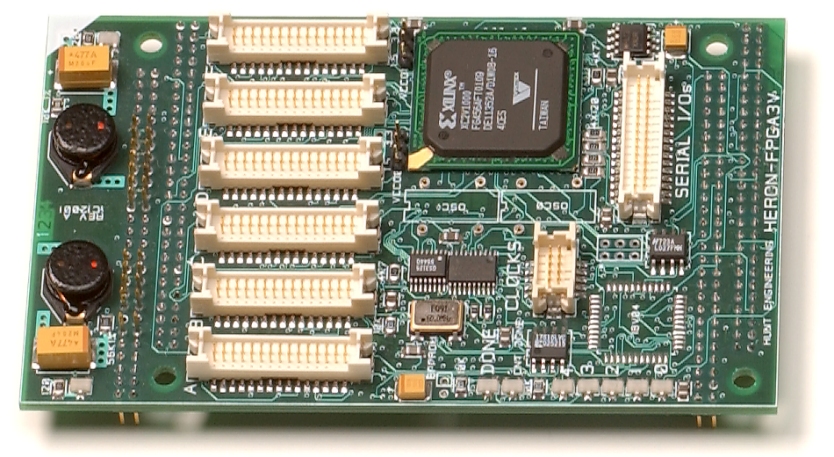
Digital Input with the HERON-FPGA3 Module
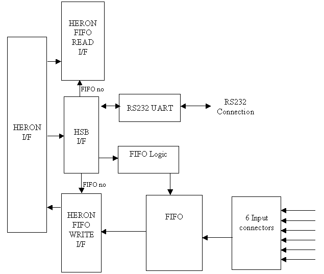
- Standard IP to provide 84 input lines, which are strobed into the module as six groups of 14
- Standard IP to provide custom I/O capability
The input connectors have 15 digital inputs each. For each connector the top (15th) bit is used as a strobe to clock data into the module. A rising edge of this clock signal is used to register the other 14 inputs from that connector. Each time a strobe is received, the values of the other 14 bits are first registered, and then written into the HERON FIFO as part of a 32 bit word. The channel number that has received the data is indicated in that word, along with an error bit.
The input buffers used in the FPGA design are LVTTL, so all inputs including the clock must be 3.3V signals that meet an input low level of 0.8V and an input high level of 2.0V. On the HERON-FPGA3V these signals must not be driven with 5V levels, but the HERON-FPGA3S is 5V tolerant.
The speed at which the other end of the FIFO is read will affect how fast data can be strobed into the module. If the strobes occur at a rate higher than the FIFO is being emptied at the other end, an overflow will occur and data will be lost. User LEDs are used to indicate that this has occurred. The event is latched and held for 0.1s so that the LED will be visible even if the event only occurs for a very short time.
This IP allows the use of HERON- FPGA3 for a custom I/O capability.
Functional Block Diagram
|
(documents open in new window) |
|||