Home>>Products>>IP for HERON-FPGA modules>>SDRAM FIFOs with HERON-FPGA12
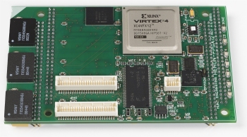
Create SDRAM Based FIFOs with the HERON-FPGA12 Module
- Standard IP that you can download to an HERON-FPGA12 module to create a large FIFO with the memory interface of the DDR SDRAM providing the storage for the FIFO
- VHDL sources so that you can add your own FPGA design to this interface which uses only a small proportion of the FPGA resources
- Highly suitable for applications requiring buffering between high speed data sources
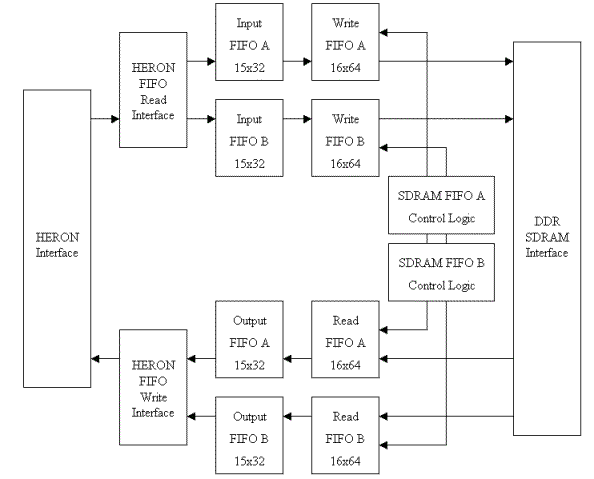
The DDR memory of the HERON-FPGA12 enables high speed data storage with access speeds of 1.6Gbytes/sec possible per bank between the DDR and the FPGA. The data rate is demonstrated by the example.
In this example the 128Mbytes of DDR memory on the HERON-FPGA12 is used to
create a single 128Mbyte FIFO that is interfaced between one HERON input FIFO
and one output FIFO.
This example is especially suitable for applications that require buffering
between high speed data sources (e.g. A/D converters of I/O modules) and slower
non-real-time host PC interfaces such as PCI
Functional Block Diagram
All I/O modules have options for cables and clocks. Please see our Cables & Clocks policy for more details!
![]() Print friendly version of HERON-FPGA12 Datasheet
Print friendly version of HERON-FPGA12 Datasheet
(documents open in new window)